
Why do reticles matter more as chip nodes shrink?

As semiconductor devices continue to shrink, reticle quality plays an increasingly important role in yield and process control. At advanced nodes, a defect that might once have been insignificant can affect thousands of devices before it is detected.
At the same time, EUV lithography has made masks more complex to manufacture and inspect. As feature sizes shrink and process margins become tighter, mask quality has a greater influence on yield and process control.
What does a reticle do in photolithography?
In semiconductor lithography, the reticle carries the circuit pattern for a single process layer. During exposure, light passes through or reflects off the reticle and projection optics transfer that pattern onto photoresist-coated wafers, typically at four times reduction.
Every transistor, via and metal interconnect on a finished chip begins as a feature on a reticle. Any defect present on the mask therefore has the potential to be reproduced throughout production.
The terms reticle and photomask are often used interchangeably. Historically, photomasks covered an entire wafer at 1:1 scale, while reticles contained a single exposure field that was stepped across the wafer.
Today, reticle is generally the more accurate term for masks used in modern step-and-scan systems.
Read more: How are reticles made
Why shrinking nodes increase the importance of mask quality
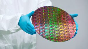 As feature sizes shrink, defect tolerance shrinks with them. A variation that may have been acceptable on a larger feature can become yield-limiting at advanced nodes.
Manufacturers must also manage focus variation, exposure dose, resist performance, etch variation and overlay accuracy within increasingly tight process margins. As process tolerances tighten, mask-related variation becomes increasingly important.
Mask errors become more significant because advanced lithography processes operate within tighter process margins. This places greater emphasis on pattern accuracy, defect control and metrology before a mask enters production.
Why a single defect can have a large impact
A defect on most optical components affects only the system in which it is installed. A defect on a reticle can be replicated across every wafer exposed with that mask.
A printing defect appears in the same location on every affected die, potentially resulting in performance issues or device failure. The cost extends beyond scrapped wafers and can include replacement masks, lost tool time and production delays.
For this reason, advanced semiconductor manufacturers invest heavily in mask inspection, qualification and monitoring.
Why EUV makes reticles more challenging
The move to extreme ultraviolet lithography introduced a different set of challenges for mask manufacturing.
Unlike previous lithography systems, EUV operates at a wavelength of 13.5 nm. At this wavelength, conventional transmissive optics are no longer practical, so the optical system relies on reflective components operating in vacuum.
The reticle itself becomes a precision mirror rather than a transparent mask. It consists of a multilayer reflective structure with a patterned absorber on the surface.
This design introduces defect mechanisms that differ from those encountered in conventional transmissive masks. Irregularities within the multilayer structure can affect the behaviour of reflected light and influence the printed pattern. Detecting and characterising these defects requires specialised inspection techniques, contributing to the complexity of EUV mask qualification.
The reticle is also illuminated off-normal, creating imaging effects that must be considered during mask design. Pellicles remain important for contamination control, but their use is more challenging than in DUV systems because any material placed in the optical path reduces the already limited amount of available light.
More layers increase defect risk
Advanced semiconductor devices require large numbers of lithography layers, each with its own reticle and alignment requirements.
Every additional layer introduces another opportunity for defects, critical dimension variation or overlay error. Maintaining pattern fidelity across every layer becomes increasingly challenging as device complexity grows.
The role of substrate quality and metrology
The quality of a reticle or patterned substrate begins before the pattern is written.
Flatness is important because any distortion can affect overlay accuracy. Surface quality and cleanliness are equally important because features present on the mask can appear in the printed image. For transmissive masks, transmitted wavefront error is another key consideration, as the mask forms part of the optical path.
These requirements are not limited to semiconductor manufacturing. Similar considerations apply to photonics, microelectromechanical systems (MEMS) and compound semiconductor fabrication.
Metrology provides the data needed to verify that patterned substrates meet specification before they enter production.
At Knight Optical, flatness, irregularity and transmitted wavefront error are measured using a Zygo Verifire XPZ phase-measuring interferometer. Pattern geometry and feature placement are verified using a Starrett AV300 measurement system. Components are also visually inspected to customer and application requirements, including ISO 10110 and MIL-PRF-13830B specifications where required.
Quality as a cost-control measure
Detecting defects before production helps reduce the cost and disruption associated with rework, scrap and process interruptions.
For this reason, semiconductor manufacturers rely on inspection and qualification throughout the life of a mask rather than treating quality control as a single incoming inspection step.
The same principle applies to lower-volume manufacturing, research environments and specialist photolithography applications. Identifying potential issues before production starts helps reduce downstream costs and minimise disruption.
Increasing demands on mask quality
Future lithography platforms are expected to require tighter control of mask fabrication, inspection and metrology.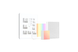
Higher numerical aperture EUV systems, increasingly complex mask designs and more advanced correction techniques all require greater precision throughout the manufacturing process.
As feature sizes continue to shrink, reticle quality becomes more closely linked to yield.
Defects that may have been acceptable at larger geometries can become yield-limiting at advanced nodes, making inspection and metrology an essential part of the manufacturing process.
Knight Optical provides precision patterned optical components and supports customers with in-house metrology and inspection capabilities.
To discuss requirements for photolithography, inspection or other precision optical applications, please contact our technical sales team: [email protected]
Read more: Optical lenses in semiconductor lithography