
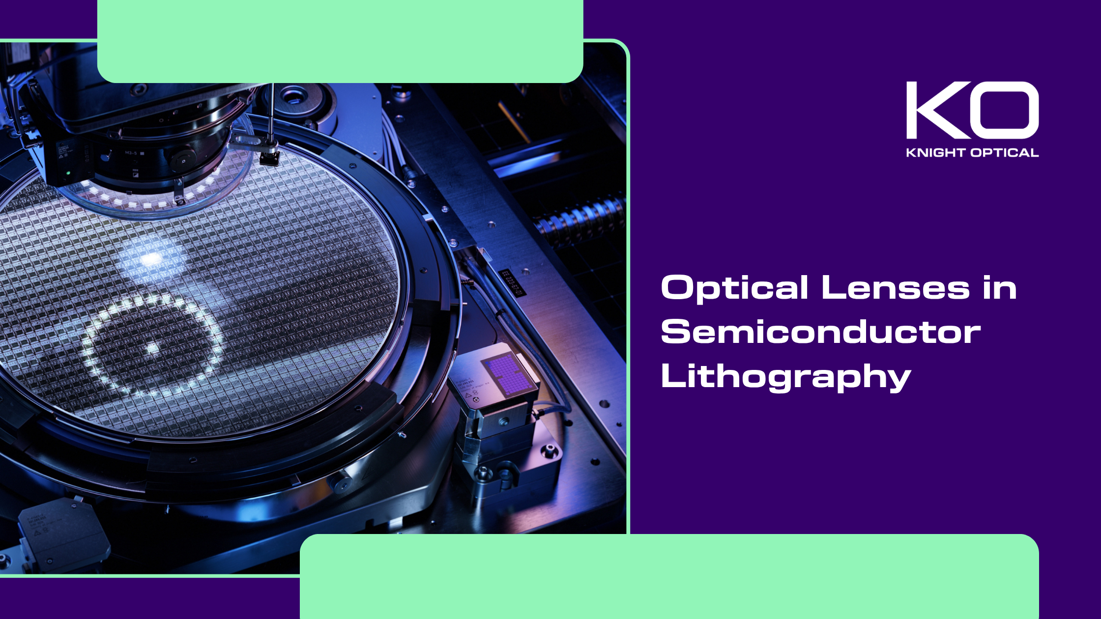

Optical lenses in semiconductor lithography

Every microchip used in smartphones, computers, vehicles, medical equipment, communications networks and industrial systems is patterned using light. The billions of transistors on an advanced chip enable faster processing, greater memory density and improved device performance. Yet none of this would be possible without precision-manufactured optical components, particularly lenses, which ultimately determine the smallest features that can be printed in semiconductor lithography.
Semiconductor lithography (also known as photolithography or optical lithography) requires a precise optical path. Light from the source is conditioned and homogenised by illumination optics before reaching the reticle (a template carrying the circuit design, sometimes referred to as a mask). Projection optics reduce the reticle image to about a quarter of its original size onto a photoresist-coated wafer. The exposed resist is then developed, and the pattern is etched into the wafer, with the cycle repeating layer upon layer, and numerous exposures building up per chip. Exposure wavelengths depend on the lithography platform: 365 nm for mercury-vapour lamp i-line systems, and 248 nm (KrF) and 193 nm (ArF) for deep ultraviolet (DUV) excimer laser systems.
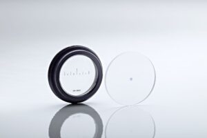
The role of lenses in semiconductor lithography
Optical lenses are included in both the illumination and projection stages of the optical chain.
In the illumination stage, lens assemblies need to control how evenly and from which angles light strikes the reticle. This shapes the image contrast at the wafer.
For projection, resolution depends on wavelength and numerical aperture (NA), which measures how much light the lens can gather and focus. The shorter the wavelength and the higher the NA, and the finer the feature that can be achieved. The precision of those lenses matters, too. Projection lenses contain dozens of elements corrected to nanometre-level wavefront accuracy.
Challenges at UV wavelengths
Because conventional optical glass (such as N-BK7) absorbs DUV, lenses for semiconductor lithography are typically fabricated from UV-grade fused silica and calcium fluoride.
Due to the limited number of transmitting substrates, DUV lenses can’t be colour-corrected to counter chromatic aberration as visible optical components can be, so excimer lasers are line-narrowed instead.
Laser energy presents its own problem: A fraction is absorbed, subtly distorting lens elements during high-volume exposure, so low-absorption materials are essential considerations at the specification phase. Each lens surface also carries antireflective (AR) coatings to preserve transmission and contrast.
Alignment and overlay are critical in semiconductor lithography. Successive layers must register to within a few nanometres, meaning alignment optics (including gratings, beamsplitters and other detection components) and positioning mechanisms are just as important as the projection lenses themselves.
Why EUV relies on mirrors instead of lenses
While immersion lithography uses water between the wafer and the final lens to push numerical aperture (NA) above 1, extreme ultraviolet (EUV) lithography operates at a wavelength of just 13.5 nm. At these wavelengths, conventional lens materials absorb the light, making refractive optics impractical. Instead, EUV systems rely entirely on reflective optics, using precision mirrors coated with multiple alternating layers of molybdenum and silicon to efficiently reflect and focus EUV light.
Precision optics across your supply chain
Beyond the semiconductor lithography system itself, microchip production leans on optics at almost every stage, and performance rests on the calibre of those components.
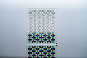
Our portfolio of stock and custom-made precision optical lenses is strengthened by our parent company’s patented microlithography expertise. Torrent Photonics’ semiconductor-style mask aligners handle wafers up to 8 inches and, with dedicated wafer fabrication cleanrooms, Torrent produces micropatterned filters at wafer scale.
To find out more about our optical lenses for semiconductor lithography, contact our technical sales team today.